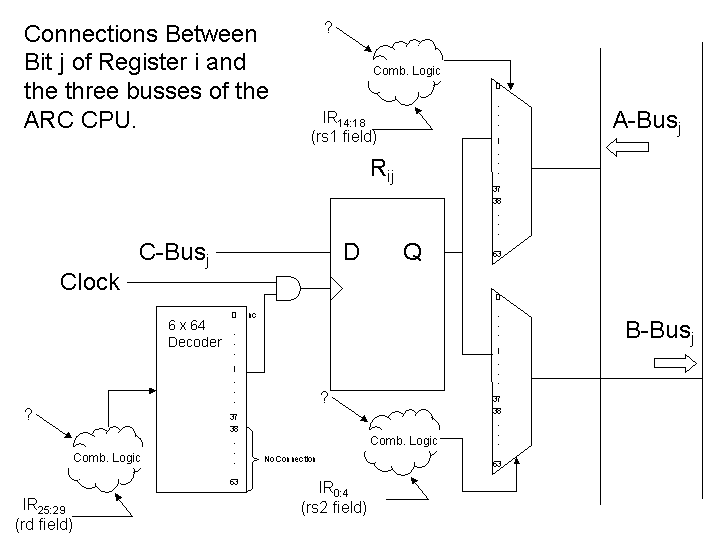
The class for November 5 went over how to connect the flip-flops in the ARC registers to the wires of the A-Bus and B-Bus using two 1068x32 multiplexers. (The 38 32-bit registers in the ARC CPU would normally becalled a "register bank" or a "register file. A "file" in this context has nothing to do with disk files at all.) In that class, we also introduced the idea that the wires of the C-Bus are connected to the D inputs of all the flip-flops in the register file, and that which register actually gets loaded can be controlled by having an AND gate for each register that controls whether clock pulses actually get to the register's flip-flops or not.
Your assignment is to draw a diagram that shows all the connections between the jth bit of register i and the three busses of the ARC datapath. That is, your diagram is to show one flip-flop, how it connects to the multiplexers for the A and B busses, where the control inputs to those multiplexers come from, where the D input of the flip-flop comes from (which wire of the C bus), where the clock input of the flip-flop comes from (a decoder), and where the inputs to that decoder would come from. Use a "cloud of logic" for the control inputs to the multiplexers as we did in class on the 5th, and show which bits of the IR would go into each of those three logic clouds, as well as how many wires go from the IR to each cloud and from each cloud to its associated multiplexer.
Draw your answer as neatly as you can on a piece of paper, and hand it in on the due date. If your answer isn't ready by class time, you can slip it under my office door (SB room A-222) any time before 8:00pm.
