Send me a single email with the two attachments described below
by midnight on the Due Date. The Subject line of your mail must
say, "CSCI-343 Assignment 4" and your mail message must start with
your name and ID number.
Use CircuitMaker to construct a clocked D latch using only AND,
OR, and Inverter gates. Use two switches for the D and clock inputs.
(Don't use a pulser for the clock for this exercise.) Attach
testpoints to the clock, D, Q, and ~Q wires in the circuit, and enable
the waveform window by pressing F12. Single step through the circuit,
setting the values of D and Clock as you go along so that you
demonstrate the effects of four clock pulses as follows:
The leading edge of the first clock pulse should turn the
latch on if it is not already on.
The leading edge of the second clock pulse is to turn the
latch off.
The latch is not to change state during the third clock
pulse.
Use the fourth clock pulse to demonstrate that the latch will
change state during the clock pulse when the value of D changes.
In addition, demonstrate that changing the value of D between clock
pulses has no effect on the state of the latch.
Go to the File->Export->Options menu item and be sure the settings
are to export as a "Window Metafile" and that the "Color" option is
set. (Windows Metafile format is more compact than bitmaps.) Set the
LED/Lamp display option to show the state of the LEDs to match their
state in the simulation, although that really doesn't matter for this
assignment.
Now use the File->Export Menu to export the circuit as
graphic, and again to export the waveforms as graphic. When you save
them make the two file names include both your last name and either
"ckt" or "waves" as part of their names. For example, I would save
the two files as "vickery_ckt.wmf" and "vickery_wave.wmf." Attach
these two wmf files to your email message that you send
me.
You must use these file naming conventions to
receive credit for this assignment.
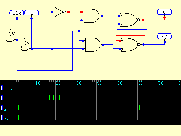
As you can see from the circuit below I meant to allow
you to use NOR gates for this design!
The oscillation at the beginning of the waveform is typical of
what will happen if the simulation starts with clock false: both NOR
gates will start off false, which will cause both to go true, which
will cause both to go false again, etc. The problem resolves once
Clock goes true the first time. "Real" sequential circuits often
have a special signal that is is generated automatically when power
is first applied, and this signal will be connected to extra inputs
in all the flip-flops to put them into known initial states (either
zero or one).

